Lots of players are getting into the “wide-but-slow” business in optical interconnects. Arm has serious AI CPU demand, but can they build chips fast enough? And other easy reading bits and bobs.
Let’s hit it.
Thanks for being one of our first fans! We’re up to 750!
Quick hits, high signal. Takes from semi industry experts. Sign up for free daily updates!
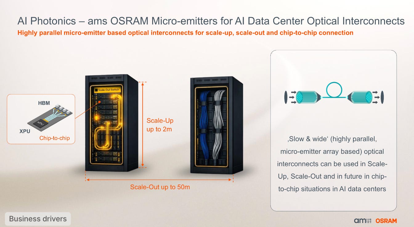
ams OSRAM bets on “slow and wide” parallel optics for the AI rack
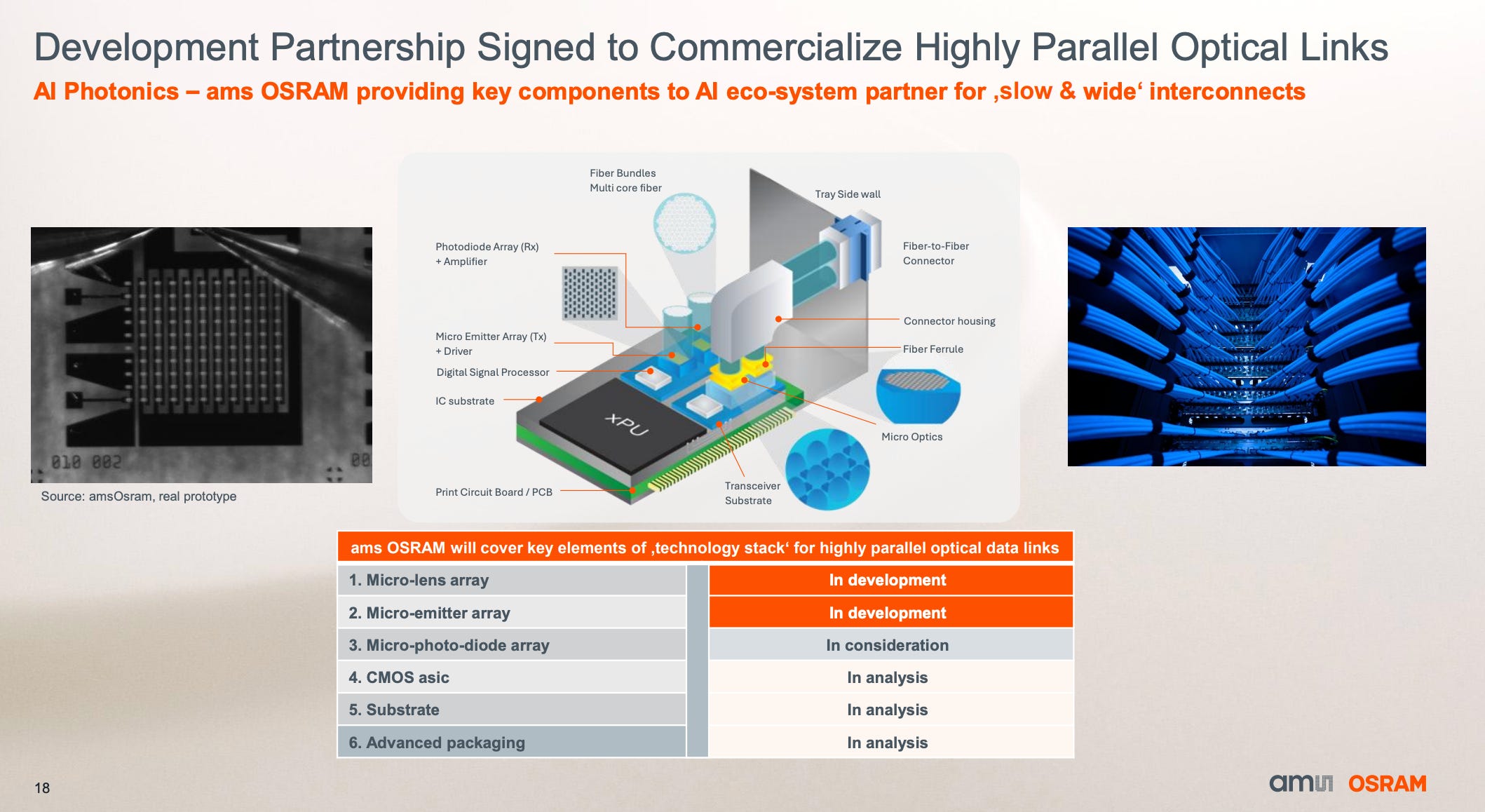
ams OSRAM signed a development agreement with a “leading AI data center infrastructure partner” to commercialize what the company calls “slow and wide” optical interconnects: highly parallel micro-emitter arrays running at 8 gigabit per channel across hundreds of parallel channels.
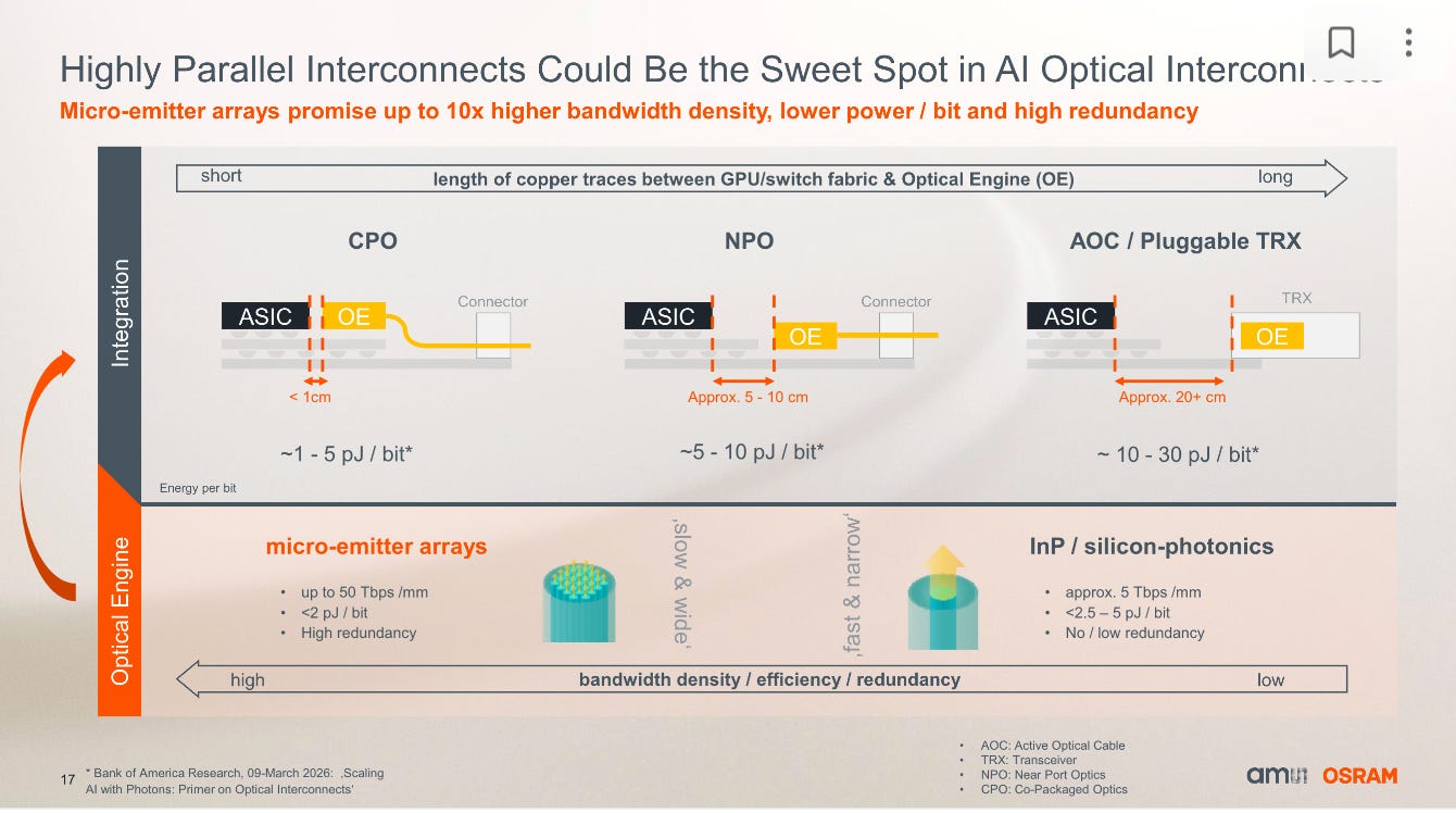
Most optical interconnects are “fast and narrow” and accelerated by power-hungry serializers and deserializers. It seems Osram is building the inverse: drop the SerDes, replace serial speed with parallel channels, and transmit light pulses at chip speed across an emitter array. CFO Rainer Irle said the initial focus is on shorter-distance scale-out interconnects (rack to rack), then scale-up within racks replacing copper over distances up to several tens of meters, and eventually chip-to-chip connections between GPUs and HBM.
ams OSRAM gave specific power numbers for the alternatives. Today’s pluggable transceivers and active optical cables consume up to 30 picojoules per bit. Near-port optics gets to 5 to 10 pJ/bit. Co-packaged optics targets 1 to 5 pJ/bit. The slow-and-wide approach achieves low pJ/bit not by moving the engine closer to the ASIC but by removing the power-hungry SerDes entirely.
The other claimed advantage is inherent redundancy: with hundreds of parallel channels, single-emitter failures degrade gracefully rather than knocking a link offline, which matters for hyperscaler uptime SLAs.
The partner is not exclusive. Rebel: “It’s not only on a similar integration level that we are speaking, but basically we’re speaking with everyone.”
On revenue: Osram said the AI-datacenter opportunity is “a EUR 3-digit million opportunity in 2030 and beyond, with a gradual ramp” if the company supplies just emitters, and could be “obviously a much higher number” if the program expands to photodiodes, drivers, and amplifiers. First revenue is targeted for “before 2030, hopefully before 2029.”
But then I though maybe this based on VCSEL arrays? ams OSRAM’s VCSEL business runs back through the OSRAM Opto Semiconductors side, including Apple Face ID dot projector, smartphone proximity sensors, automotive LiDAR sources, and datacom transceiver lasers. Touched on this the other day at Chipstrat:
And ams OSRAM management used “microLED” elsewhere on the same call when describing smart-glasses displays, but deliberately switched to “micro-emitter array” for this AI program… so maybe VCSELs?
But then a friend looked at the image in the slides and said it looked like uLEDs:
Vik: InP lasers for shorter reach is overkill, and supply chain is F-ed. Lots of reasons to go either microLED or VCSEL arrays. Question is which one?
Arm Has the Demand. Does The Supply Chain?
Per Arm’s recent earnings call, AGI CPU customer demand has more than doubled since the launch six weeks ago. Yet Arm is keeping the FY26 revenue outlook flat while it secures the supply needed to fulfill the new pipeline.
Jason Child, CFO:“As Rene mentioned, customer demand for the Arm AGI CPU is very strong. We now have line of sight to more than $2 billion of demand across fiscal ‘27 and ‘28. However, we are maintaining our outlook of $1 billion while we pursue supply chain capacity, and we still expect the first revenues from production chip sales to land in the fourth quarter of this fiscal year.”
Can Arm actually build the chips in time? It’s “working around the clock” to pull it off:
Rene Haas:“The number that we talked about at end of March was supply in place to support $1 billion of demand, and that includes memory, that includes wafers, that includes packaging, that includes access to test equipment. So for the $2 billion, we are now in the process of securing supply to support that. And the teams are working around the clock to make sure we can find the right answers for our customers.”
Building chips has much lower margins than selling IP… but if you build the IP already, it might not be as expensive as you’d think for Arm to take CSS to final taped out chip:
Jason Child:“The most expensive part of developing a chip is really the compute die, which really is effectively kind of the CSS. So we’re able to leverage that, and that automatically makes this business much more profitable as a stand-alone chip business given that we get that work as part of our IP business already. So the incremental costs and OpEx that we’re having to add to the chip business is not that significant. It’s a team that’s in the dozens of people, not hundreds. And so you can assume that it’s operating profit positive next year.”
Dozens of people, not hundreds!
Austin:The existing IP business is paying a large portion of the chip development cost, that’s pretty sweet. Or you could look at it from the inverse angle: the chip business is funded by licensing its internal IP to external customers too.
Key Data
We covered the “memory tax” on a Semi Doped episode. This chart shows just how true it is.
These things are beautiful to look at. See the honking black cables between racks? That’s scale out. Anyway, this is Meta Catalina from a year ago, Custom build based on GB200. It uses a 1:1 CPU:GPU ratio.
TIL: The Semiconductor Industry Exists Because One Guy Got Annoyed by Dust
Everyone knows the transistor, but almost nobody knows the environment required to build one. Before 1960, “clean rooms” were a disaster. Even the most advanced labs were filled with over 1,000,000 particles of dust per cubic foot - a literal minefield for microscopic circuitry.
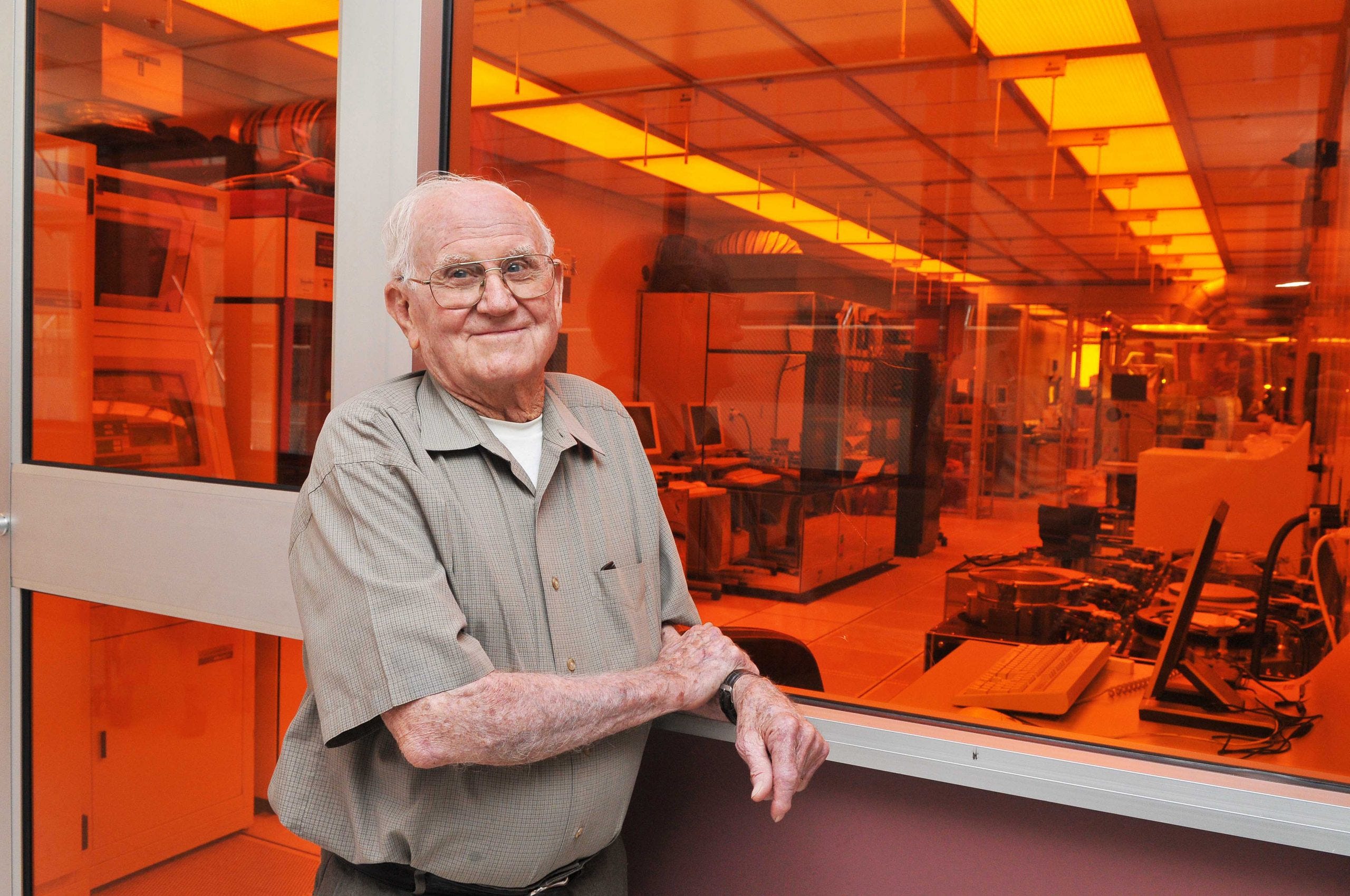
Enter Willis Whitfield (fondly called Mr. Clean), a physicist and son of cotton farmers who learned engineering by fixing farm equipment. While working at Sandia National Laboratories, Whitfield realized the industry’s fatal flaw: they were trying to trap dust instead of removing it.
His “Aha!” moment came on an airplane, where he sketched a solution in five minutes: Laminar Flow. His insight was brilliantly simple: stop fighting the particles and instead “let the air be the janitor.” By blowing a constant, ultra-filtered curtain of air from the ceiling to the floor, he effectively swept the room clean every few seconds.
The results were so radical they were scary. His prototype brought the particle count from 1,000,000 down to 750. It was so clean that fellow scientists initially thought his measuring instruments were broken!
Despite enabling a global industry now worth hundreds of billions, Whitfield never got rich. Because the U.S. government placed the patent in the public domain. He later helped NASA sterilize spacecrafts, but his true legacy is the “invisible infrastructure” of the modern world. From TSMC’s fabs to your phone’s OLED display, we are all living in a reality made possible by a five-minute sketch and a man who hated dust.
Willis Whitfield, aka, Mr. Clean. Source: Sandia Labs.
Thanks for reading! This post is public so feel free to share it.